ASML spinout Invisix raises €20M to peer inside hidden chip structures

▼ Summary
– Invisix, an Eindhoven startup spun out of ASML, has raised €20 million to solve the problem of inspecting complex 3D chip structures that optical tools cannot resolve.
– The oversubscribed seed round includes Hitachi Ventures, Transition Ventures, imec.xpand, Doosan Investment Co., and an anonymous tier-1 semiconductor manufacturer, likely Samsung.
– Invisix uses high-harmonic generation, a Nobel Prize-winning physics technique, to produce soft x-rays that create a rich 3D signal, combined with algorithms to non-destructively reconstruct internal chip structures.
– The company licensed over a decade of soft x-ray technology from ASML and demonstrated its approach in 2023 with Intel and imec, measuring gate-all-around transistors.
– Invisix will use the funds to grow its team, build its first shippable system, and run customer demonstrations from a new Eindhoven cleanroom.
Modern chips have a measurement problem that borders on the philosophical: they have grown too complex to be properly seen. As logic and memory devices stack into three dimensions and shrink to just a few nanometres, the optical tools that inspect each layer can no longer resolve the structures buried within.
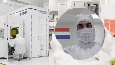
Invisix, an Eindhoven startup spun out of ASML, has raised €20 million to solve that blind spot. The oversubscribed seed round attracted Hitachi Ventures, Transition Ventures, imec.xpand, Doosan Investment Co., and, as the company puts it, a tier-1 semiconductor manufacturer. That anonymous backer is a powerful signal in an industry where chipmakers rarely invest in tools they do not intend to use. Earlier reporting has suggested Samsung may be taking a stake as it works on yields for its 2nm process. Invisix will use the capital to expand its team, build its first shippable system, and run customer demonstrations from a new cleanroom in Eindhoven.
The problem Invisix addresses is fundamentally a yield problem, which in semiconductors is a money problem. Building a chip is a layer-by-layer process. If you cannot confirm a layer printed correctly before adding the next, you are effectively flying blind. Today, that often means slow, expensive, and sometimes destructive checks, like slicing apart a finished wafer to inspect it. In a business where a marginal yield gain is worth billions and the race is won by reaching a new node first, that gap is costly.
Invisix’s solution borrows the logic that drove lithography itself: to see smaller things, use smaller wavelengths. Its system relies on high-harmonic generation, the physics recognized by the 2023 Nobel Prize in Physics awarded to Pierre Agostini, Ferenc Krausz, and Lund University’s Anne L’Huillier. A short-pulse laser excites noble-gas atoms until they emit soft x-rays across many wavelengths simultaneously, producing a richer 3D signal than a single-colour laser. The company pairs this with reconstruction algorithms and machine learning to rebuild a device’s internal structure without destroying it.
What makes this bet unusual for a seed-stage hardware company is how much risk has already been retired. Invisix licensed a substantial soft x-ray technology package developed over more than a decade inside ASML. Its team is stocked with veterans of that programme alongside senior hires such as COO Roald Dogge, formerly of contract manufacturer NTS. The company says it publicly demonstrated the approach in 2023 with Intel and imec, measuring features in gate-all-around transistors, among the hardest targets for existing metrology.
The wider context is a continent trying to hold onto the parts of the chip supply chain it leads. The Netherlands is home to ASML, and a cluster of Dutch and Belgian deep-tech funds, including imec.xpand, now backs the startups forming around it. Invisix has the testbench, the pedigree, and the cleanroom. The test ahead is the unforgiving one for any tool company: turning a demonstration into a system a fab will run at volume.
(Source: The Next Web)