SMIC N+3 vs Intel 18A: Which Has the Smaller Metal Pitch?
▼ Summary
– SMIC’s N+3 process, used in Huawei’s Kirin 9030, achieves a transistor density of 113.4 MTr/mm², slightly above TSMC N6 (107.7 MTr/mm²), but relies on aggressive DUV multi-patterning without EUV, increasing complexity and cost.
– The Kirin 9030’s CPU performance trails current flagships; its prime core is roughly on par with a 2021 design, while Apple’s M5 P-core is 2.7× faster in absolute integer performance.
– SMIC N+3 uses a 32.5 nm local metal pitch (M0), tighter than Intel 18A’s 36 nm in Panther Lake, but this metric alone does not indicate superior process maturity due to trade-offs in routing and process control.
– Huawei’s roadmap includes LogicFolding, a 3D stacking approach to shorten wires and recover density, targeting prime core frequencies of ~5 GHz by 2031, though the Kirin 9030 does not use this technology.
– Export controls have not halted Huawei and SMIC’s progress, but have forced a shift toward domestic EDA tools and architectures, with SMIC licensing its processes to other Chinese fabs, diffusing manufacturing knowledge.
Nearly four years ago, we reported that SMIC had begun shipping 7 nm (N+1) chips. Today, the Chinese foundry is delivering its third-generation 7 nm (N+3) process inside Huawei’s Kirin 9030, featuring a minimum metal pitch of 32.5 nm. That is roughly 10% tighter than the 36 nm minimum metal pitch found in Intel’s latest Panther Lake CPUs on 18A.
That headline is accurate, but it is also a cherry-picked metric. N+3 achieves density comparable to TSMC N6 through aggressive DUV multi-patterning and design-technology co-optimization (DTCO), but the trade-offs are significant: higher complexity, lower efficiency, and more difficult process control.
These findings come from our reverse engineering and teardown, which covers SMIC’s N+3 process technology, Huawei’s packaging, memory, architecture, and more. SemiAnalysis has spent the last year and a half building a state-of-the-art teardown lab in Oregon, capable of analyzing the world’s most advanced and important chips. We have already generated revenue from advanced datacenter chip teardowns, including our recent reverse engineering of a major TSMC customer’s COUPE CPO optical engine and EIC 3D stack.
This is the first public report from the SemiAnalysis Teardown Engineering & Evaluation Lab (STEEL). The lab is scaling up aggressively, and we are excited to announce it publicly. The timing is somewhat inconvenient for TechInsights, which is private equity-owned and currently being sold, having enjoyed virtually no credible competition for decades. That lack of competition has led TechInsights to underinvest in CAPEX.
SemiAnalysis already exceeds TechInsights in revenue, despite having no venture or private equity backing and being founded only six years ago. Because we are founder-led with no external investors, we move faster, build faster, and can release client chip teardowns for free on a regular basis, while focusing on datacenter work for our major clients.
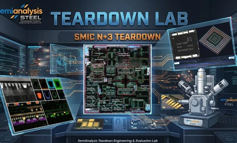
Here is the first public image from our lab: the HiSilicon Kirin 9030 Pro SoC.
This report details our teardown of the Kirin 9030 and our findings on SMIC’s N+3 process, the most advanced node in China. For comparison, we also show our teardown of the MediaTek Helio G99, built on TSMC N6. Through this comparison, we can see the impact of export controls: SMIC N+3 and TSMC N6 are comparable nodes, but one is heavily restricted while the other has free access to the West’s most advanced equipment.
The results show both China’s progress and its constraints. SMIC N+3 reaches TSMC N6-class logic density, but it requires far more aggressive DUV multi-patterning, so it does not match N6 on process maturity or cost. The Kirin 9030 Pro performs similarly to three-year-old Android flagships and trails far behind current flagship SoCs from Apple, Qualcomm, MediaTek, and Samsung. The efficiency gap is even wider.
Export controls have not stopped Huawei and SMIC from shipping advanced silicon, but they have forced a different path. Without EUV, SMIC relies more heavily on DUV multi-patterning, DTCO, and increasingly complex integration. The roadmap continues forward through tighter design rules and backside power, but each step adds cost and process risk. Huawei’s τ scaling and LogicFolding offer another path: stacking active logic and recovering density through advanced packaging and system-technology co-optimization (STCO).
Die Shot & Floorplan
To understand the Kirin 9030, we must first understand Huawei’s SoC history. HiSilicon is Huawei’s chip design arm, responsible for the Kirin smartphone SoCs, Kunpeng server CPUs, Ascend AI accelerators, and networking silicon.
Before export controls, Huawei was one of TSMC’s largest customers. It was the only customer on TSMC’s first EUV node, N7+, and among the first on N5, alongside Apple. That ended in late 2020. Huawei switched to Qualcomm SoCs in its flagship smartphones, though export controls limited them to 4G-only variants.
In late 2023, Huawei returned to in-house silicon with the Kirin 9000s, a successor to the Kirin 9000, fabricated on SMIC N+2 instead of TSMC N5. In the following years, they released the Kirin 9010 and 9020 on the same N+2 process. These chips used Huawei’s in-house TaiShan CPU cores and Maleoon GPU.
We have not torn down a Kirin 9020 ourselves, so the predecessor die shot comes from Kurnal. The die shots show how Huawei spent its silicon budget: which functional blocks are where, and how their areas compare to the predecessor.
First, a quick guide to the major blocks on the die.
The total die area is nearly identical, but the 9030 uses that area more aggressively. A denser process lets Huawei fit an extra middle CPU core, more GPU and NPU cores, and larger caches into the same footprint.
In contrast, the Helio G99 is a much smaller, low-cost SoC built for budget smartphones rather than a flagship device. While the Kirin 9030 is roughly 140 mm², the G99 is only about 29 mm², roughly one-fifth the area. The underlying TSMC process technology, however, is directly comparable as a baseline for analyzing SMIC’s.
Architecture & PPA
The Kirin 9030 is an evolutionary refresh, not a clean-sheet design. Its CPU, GPU, and NPU cores carry over the 9020’s families, and the gains come from three levers: the SMIC N+2-to-N+3 process step, DTCO and floorplan work, and incremental microarchitecture. Area is where the first two show up, and the 9030 scales well there. Performance and efficiency are the harder test. Huawei’s design holds up better than its node would suggest, but the chip still trails, both because N+3 sits behind the leading-edge nodes and because its cores, while competent, remain a few generations behind the newest designs.
The new prime core is an incremental update. The main changes are a 10% frequency increase from 2.5 GHz to 2.75 GHz and a doubling in the L2 cache from 1 MiB to 2 MiB. Despite the increased cache, the core size decreased by 7.6%. Excluding the private L2 cache, the core size decreased by 21%. This is a large reduction for an incremental node.
Compared with the TaiShan New V120 core in the Kirin 9020, the Kirin 9030’s middle core is almost unchanged architecturally, yet each core shrinks by roughly 22%. Most of that comes from the move from N+2 to N+3, with layout changes likely accounting for the rest.
Visually, the most noticeable change is the increase from 3 middle cores to 4. There is also a 20% increase in the shared L3 cache of the big cluster. This helps improve multi-core performance without sacrificing much area.
Even with each core shrinking, the big CPU cluster’s total area is essentially unchanged. The per-core savings went back into an additional middle core and larger caches.
The tiny cores shrank less than the prime core (excluding its L2 cache) and less than the middle cores. This is likely because fixed overhead is a larger share on a small core. We cannot resolve any architectural changes from the die shot alone, but the per-clock and efficiency gains shown below point to more than pure process and layout scaling. The area reduction was offset by a doubling of the shared L2 cache from 2 MiB to 4 MiB, leaving the total tiny CPU cluster area slightly larger.
Area is the easiest improvement to see from a die shot, but it is only one part of PPA (power, performance, area). For modern logic, power and performance matter just as much, and often more. Since Dennard scaling broke down in the mid-2000s, voltage and frequency have not scaled in step with transistor dimensions, so each node has had to fight harder for gains in performance and efficiency.
The starkest comparison is not Kirin 9020 versus Kirin 9030 Pro. Apple’s efficiency cores run circles around Huawei’s prime core. Apple’s low-power core delivers 20% higher integer performance while drawing only 1 W, compared with 4.5 W for Huawei’s prime core. N+3 matches TSMC N6, but N6 is several generations old. Apple and Qualcomm build on N4 and N3P, which are denser and sit on a better voltage-frequency curve, giving them a larger transistor budget and more performance per watt.
The 9030’s own cores did improve. The middle and tiny cores gained 17% and 14% in per-clock integer performance over the 9020, with floating-point flat on the middle core and up 11% on the tiny. The tiny core improves cleanly, with performance rising while power falls and efficiency increases by 45% in integer and 24% in floating point. The middle core is mixed: integer performance rises but power rises faster, cutting integer efficiency by 7%, while lower power lifts floating-point efficiency 16%.
Per-clock gains at the same or lower frequency are microarchitectural, so the cores are tuned, not just shrunk. Both also failed to hold their rated maximum frequencies, pointing to thermal, power, or stability limits. Per clock, the middle core sits around Arm Cortex-A720 and the tiny core near the Cortex-A520; absolute performance trails because Huawei clocks them much lower.
The prime core is roughly Cortex-X2 class per clock, a 2021 design. Apple’s 2020 M1 Firestorm core is still 35% higher per clock and 57% faster in absolute integer performance at a similar 4.5 W. The current leading edge is further ahead: the Apple M5 P-core is 60% higher per clock and 2.7× faster, the Arm C1 Ultra is 45% higher and 2× faster.
Matching older high-end cores per clock is a genuine design achievement. What Huawei cannot match is the voltage-frequency curve and transistor budget of leading-edge nodes, which let Apple, Qualcomm, and others spend more transistors in the same area on wider cores, larger caches, and deeper buffers while running at lower voltage.
Huawei’s LogicFolding roadmap is one answer, stacking active logic to recover density and shorten signal paths. We return to it later.
The GPU compute units (CUs) changed more visibly than the CPU cores, moving to a more rectangular layout for both the arithmetic logic unit (ALU) clusters and the CU overall. Even with ray-tracing support added, a CU shrank roughly 28%.
However, that shrink is offset by the increase from 4 to 6 CUs and the area outside the CUs grew 33%. Overall, the GPU cluster is larger by roughly 10%.
The GPU is where Huawei makes its biggest gains. The Maleoon 935 is not competitive with current flagships, but it is a large step up from the 920 and reaches older-flagship territory. In 3DMark, it is 70% faster in Wild Life Extreme (WLE) and 79% faster in Steel Nomad Light (SNL) than the 920; with 11% higher clocks and 50% more CUs, the roughly 67% theoretical uplift roughly matches WLE and is beaten by SNL.
It edges ahead of the Snapdragon 8+ Gen 1 in WLE and SNL, and the Dimensity 9200 and Apple A16 in WLE, but stays far behind newer parts: the Snapdragon 8 Elite Gen 5 and Dimensity 9500 are roughly 2.4–2.6× faster in WLE and 3.2× faster in SNL.
The Maleoon 935 is Huawei’s first GPU with hardware-accelerated ray tracing; there it lands slightly ahead of the Exynos 2200 and on par with the Apple A16, with current flagships up to 3.7× faster.
The Neural Processing Unit (NPU) saw the largest structural changes of any block, moving from a Lite and a Tiny core in the Kirin 9020 to a Lite and two Tiny cores in the Kirin 9030. Both core types also show significant layout changes.
This is a reversal in Huawei’s NPU design. The Kirin 9000 5G, its last flagship chip on TSMC N5, used two Lite and one Tiny core. The series of SoCs on SMIC N+2 moved to one Lite and one Tiny core, likely for area savings. With the Kirin 9030, Huawei has shifted back toward a larger multi-core NPU cluster, but the additional area goes to a Tiny core rather than a Lite core.
Memory
The Pro variant of the Kirin 9030 carries 12 GB of Samsung DRAM, with two stacks of four dies each. The dies were identified as the K4L2E165YD, a 12 Gb LPDDR5X-9600 device fabricated on Samsung’s 1a node, the fourth generation of its 10 nm-class DRAM after 1x, 1y, and 1z. 1a has shipped in volume since 2022, so this is current memory rather than older-node inventory.
The 16 GB Pro Max variants we obtained were found with both CXMT and Samsung packages. The CXMT package is marked CXDD7JEDM, with two stacks of four dies, packaged in week 45 of 2025. The inferred die dimensions from X-ray computed tomography (CT) are consistent with a known density of roughly 0.3 Gib/mm² for the CXMT G4 process, roughly equivalent to other manufacturers’ 1z processes.
Packaging
The Kirin 9030 uses a typical integrated package-on-package (iPoP) stack: multiple DRAM dies in a memory package sit above an organic redistribution layer (RDL) interposer, which sits above the SoC and package substrate. The full package is then mounted to the printed circuit board (PCB) through ball-grid array (BGA) solder bumps.
The memory package substrate is a thin bismaleimide-triazine (BT) laminate carrying the LPDDR5X stack. The organic RDL interposer over the SoC routes the PoP signals around the die and carries possible dummy thermal copper pillars. The package substrate, a thicker Ajinomoto Build-up Film (ABF) build-up over a BT core, fans the flip-chip bumps out to BGA pitch and embeds the power planes.
The whole stack is organic. The only silicon is the SoC and the LPDDR5X dies; there is no silicon interposer. Keeping it all-organic brings the package’s coefficient of thermal expansion (CTE) close to the PCB’s, reducing board-level warpage, and avoids the cost of a silicon interposer that the SoC’s bandwidth does not need.
In an iPoP stack, the memory package connects to the organic RDL interposer through an array of solder bumps. Underfill fills the gap around those bumps, adding stiffness and protecting the joints from mechanical stress. The Pro and Pro Max variants differ here, which we cover behind the paywall.
Process
The die shot and architecture tell us how Huawei allocated its silicon budget. The process tells us what SMIC can manufacture. We use the Helio G99 as the process reference for TSMC N6. Both SMIC N+3 and TSMC N6 are evolutions of previous 7 nm-class nodes.
We used targeted TEM cross-sections through logic and memory regions, imaged in both fin-cut and gate-cut directions. Each cross-section caption gives its horizontal field width (HFW), the real width of the imaged area. We start at the transistor fins, then move up through standard cells, local interconnect, and SRAM.
SMIC has not overtaken Intel or TSMC. It uses aggressive DUV scaling and DTCO to reach N6-class density, but that density does not translate into comparable performance and efficiency, for two reasons: the node gap to leading-edge nodes and Huawei’s core designs.
Fin Profile
One of the most important knobs in a FinFET process is the fin profile: the shape of an individual fin and the channel where current passes from source to drain. The ideal fin is tall, narrow, and nearly vertical. A taller fin increases effective channel width, while a narrower fin improves electrostatic control by thinning the body the gate must control. Push either too far, and the process pays for it: weaker drive current, fragile fins, taper, footing, and line-edge variation that hit yield and device variability.
The Intel 22 nm, 14 nm, and 10 nm fin cross-sections show how FinFET nodes have improved over time. 22 nm fins were a first-generation structure, relatively short, wide, and strongly tapered. The shape limits current density and reduces gate control uniformity across the height of the fin. At 14 nm and 10 nm, Intel pushed the fins taller and narrower while also making the sidewalls more vertical. Rather than shrinking the device, these changes increase the effective channel width per fin and improve electrostatic control. The trade-off is that taller fins at tighter pitches are much more difficult to manufacture.
Now, let’s compare the Helio G99 on TSMC N6 with the Kirin 9030 on SMIC N+3. Both processes are in the same class, with fin pitch of 30-32 nm on N+3 and 34 nm in our N6 cross-section. The pitch for N6 is especially interesting, as N7’s HD library is generally listed with a 33 nm fin pitch, and N6 did not shrink pitches directly. Its density gains came from DTCO instead of tighter pitches. The 34 nm pitch was stable across our sampled region and serves more as a comparison against the SMIC N+3 we have not investigated further.
Pinning down N+3’s fin patterning scheme takes more than one core unit. The CPU cores show a dense ~32 nm pitch, with the pitch between N-P fin pairs alternating between 78 and 88 nm. Logic alone may be consistent with dual-pitch mandrels of 120 and 110 nm, but this is a complex and unusual approach. Combining the pitch from the 8T SRAM, which has a more complex repeat unit, with the CPU core sequence allows us to reverse engineer the patterning steps with more confidence.
As both the logic and SRAM should share the same base grid, a single CD mandrel lithography pattern with 128 nm pitch undergoing SAQP produces a die-wide ~32 nm grid (128 nm/4), which supports the pitch sequencing seen in both logic and SRAM cells.
In the sampled cross-sections, N+3 shows a taller, narrower, higher-aspect-ratio fin than N6. The measured fin aspect ratio is ~9.5:1 on N+3 versus 7.8:1 on N6. N+3 also shows less top rounding, with an estimated radius of ~2 nm, compared with 2.8 nm on N6. Even though the fin widths differ, the ratio of top rounding to fin width tells the same story, with N+3 at 0.37 and N6 at 0.44. In a geometric sense, lower is better; a perfectly rectangular fin would have no top-rounding penalty.
These are single-digit-nanometer features measured from a handful of cuts, so treat the absolute numbers as approximate. The important result is the relative gap: N+3’s fins are consistently taller, narrower, and less rounded than N6’s.
Standard Cell
A standard cell is the basic building block of chip layout: a fixed-height row pairing one NMOS and one PMOS transistor that share a gate, tiled in a grid to build logic blocks. The key dimensions are contacted gate pitch (CGP), cell height (CH), fin count, and the lower-metal routing grid.
To measure density, we use the Bohr metric: a weighted average of NAND2 gate area (60%) and scan flip-flop area (40%). This represents a realistic mix of combinational and sequential logic. This metric has its limitations, especially for complex cell layouts like TSMC’s FinFLEX, which alternates cells with different fin counts. Even so, it is the best metric for a pure process-level comparison.
Another important measurement is the fin pitch; it refers to the distance between two fins of the same transistor. In a FinFET process, multiple fins are used in each transistor to increase the drive current and thus performance.
TSMC N6 ships both a high-density (HD) library with 2 PMOS and 2 NMOS fins per cell, and a high-performance (HP) library with 3 of each. More fins under the shared gate mean more effective channel width. HP cells switch harder at the cost of area. Designers mix the two on a die, primarily spending HP cells on timing-critical paths, and matching their PPA targets.
In the Cortex-A55 core of the Helio G99, we found a cell height of 240 nm for the HD cell. MediaTek has used HD cells in the G99 to minimize die size and thus cost. As an SoC for budget smartphones at roughly $100, this is essential.
By contrast, we found only one library in the Kirin 9030, with 2 NMOS and 2 PMOS fins. This suggests a narrower library strategy than TSMC N6, where both HD and HP libraries are widely used. This likely reflects the smaller customer base and the more constrained domestic design and electronic design automation (EDA) ecosystem.
In all three CPU cores of the Kirin 9030, we found cell heights of 228 nm, 5% smaller than on N6. This is also a reduction of 9.5% over SMIC N+2’s cell height of 252 nm.
SMIC N+3 and TSMC N6’s HD library both feature a CGP of 57 nm. For SMIC, this is a 9.5% shrink over N+2.
In the past, CGP and cell height alone may have been enough to compare transistor density. Now, however, we must consider scaling boosters and DTCO as well. SMIC’s density gain does not come from EUV. It comes from using every available DTCO booster aggressively.
First is fin depopulation: reducing the number of NMOS and PMOS fins in each cell. The first FinFET nodes started with 3 or 4 fins for each transistor. SMIC N+3 and TSMC N6 HD both use only 2 fins per transistor, trading drive strength for density.
Next is contact over active gate (COAG). By landing the gate contact directly over the active gate, instead of out over the isolation region, the cell height drops. N+3 integrates COAG while N6 does not. Our N+3 gate-cut cross-sections indicate COAG, with the gate contact sitting over the active region, while N6 shows an off-gate contact.
Last is single diffusion break (SDB). Diffusion breaks are inserted between cells in the same row to provide electrical isolation, but they also introduce local layout effects (LLE), layout-dependent shifts in electrical characteristics. In the past, a double diffusion break was used, consuming the space of two CGPs. SMIC N+3 and TSMC N6 instead use SDB, saving area but increasing LLE sensitivity. This must be controlled at the process level and accurately modeled in the process design kit (PDK) so that EDA tools can account for it.
Overall, SMIC N+3 has a transistor density of 113.4 MTr/mm², slightly above TSMC N6 at 107.7 MTr/mm². Even without EUV, SMIC has achieved density beyond TSMC’s mature N6 node which utilizes EUV.
Metal Stack
The smallest critical dimension in the teardown is M0; SMIC N+3 uses a 32.5 nm local metal pitch. That is smaller than the 36 nm M0 pitch on Intel 18A in Panther Lake. However, this does not mean that SMIC has a better process than Intel 18A or TSMC N3P. M0 is a local intra-cell routing layer. Its usefulness depends on the full interconnect stack: M1 and M2 pitch, track count, via and line resistance, design rules, mask count, overlay control, and routing flexibility.
The 32.5 nm M0 is consistent with self-aligned quadruple patterning (SAQP), whose four-population line-width loading we read coarsely as alternating widths of 21.5 to 24 nm; M1 and M2, at 38 and 40 nm, are consistent with self-aligned double patterning (SADP), a single A/B split. On TSMC N6, M0, M2, and M3 sit at a relaxed ~40 nm and are consistent with SADP-class double patterning, with no need for quadruple patterning. That said, we measure M2 for example at ~43 nm, likely inflated by sparse routing. We do not assign any specific layer to EUV from our cross-sections; the distinction we can draw is double versus quadruple patterning, not lithography wavelength.
Transistor-level density in the front-end-of-line (FEOL) sets an upper bound, but the design is ultimately limited by what the interconnect stack can route. The lowest metals are the most important for standard-cell density, but the semi-global and global layers determine how usable that density is at the block and chip level.
Two axes are commonly used for chip cross-sections: the fin-cut and the gate-cut. The micrograph above is a fin-cut and shows metals 0 through 3. This axis lets us see the even-numbered metals, with M0 right above the fins.
There are two kinds of M0 lines. The first are the power rails; these are wide wires for the VDD and VSS running horizontally at the top and bottom edges of each standard cell. The wide wires measure 55 nm across, more than double the other M0 lines. Their width minimizes resistance and reduces IR drop. The second kind are intra-cell wires, short segments within the cell that connect terminals to M1. These have alternating widths between 21.5 and 24 nm.
The M0 pitch is 32.5 nm, a 19% reduction versus N+2 and N6. At this pitch, DUV patterning requires more aggressive multi-patterning, increasing mask count, overlay sensitivity, process complexity, and cost.
M0 is below what a single DUV-defined spacer (SADP) can resolve, so SMIC cascades a second spacer step (SAQP). The cross-section reflects the cost: the M0 trenches are visibly more re-entrant (narrower at the bottom than the top) than M
(Source: Semianalysis.com)