IBM claims first sub-1-nanometer chip technology
▼ Summary
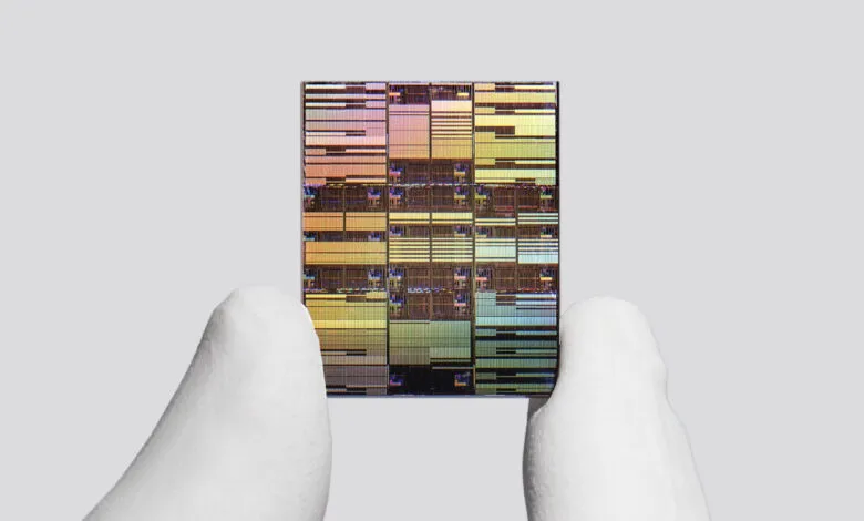
– IBM’s new chip architecture integrates nearly 100 billion transistors on a fingernail-sized chip, achieving nearly twice the transistor density of its previous generation.
– The chip technology is described as the “world’s first sub-1 nanometer chip technology” for AI data centers, improving compute performance and energy efficiency.
– IBM’s Jay Gambetta called the development a “meaningful leap forward” that could make computing more powerful without increasing energy use.
– The “sub-1 nanometer” claim refers to the 0.7-nanometer node (7 angstroms), but this does not represent actual physical feature sizes.
– The node number (e.g., 0.7 nanometer) is a marketing term, as physical chip features have not matched node names for decades, including current 3-nanometer and 2-nanometer processes.
IBM has unveiled a new chip architecture that can pack roughly 100 billion transistors onto a surface roughly the size of a human fingernail. That represents nearly double the transistor density of the company’s previous chip generation. The leap in compute performance and energy efficiency stems from what IBM calls the “world’s first sub-1 nanometer chip technology”, a development aimed squarely at AI data centers.
“It’s not just an incremental step, it’s a meaningful leap forward,” said Jay Gambetta, director of IBM Research and IBM Fellow, during an advance media briefing. He described the breakthrough as “pointing to a future where computing becomes significantly more powerful without a corresponding increase in energy.”
To understand what “sub-1 nanometer chip technology” really means, a bit of context helps. Building physically functional transistors smaller than 1 nanometer is impractical due to fundamental physical constraints. Instead, IBM’s claim rests on a new “nanostack” architecture that delivers the performance gains you would expect from a theoretical chip with sub-1-nanometer features, even though the actual physical dimensions are different.
IBM positions this technology at the 0.7-nanometer node, which it calls the 7 angstrom node (since 1 nanometer equals 10 angstroms). But these node numbers have long been decoupled from actual physical feature sizes. In the 1970s and 1980s, a chip made at the 180-nanometer node had features that actually measured 180 nanometers. That stopped being true generations ago, and it certainly does not apply to today’s cutting-edge 3-nanometer or 2-nanometer processes.
(Source: Ars Technica)