TSMC’s HBM4 Revolution: 3nm Dies to Triple Performance by 2027
▼ Summary
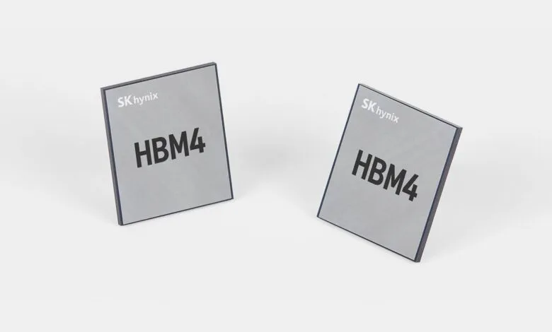
– HBM4 and HBM4E are set for 2026/2027 release, featuring a major upgrade to a 2048-bit interface and base dies built with advanced logic technologies like 3nm-class nodes.
– HBM4E will offer significantly higher bandwidth (up to 3 TB/s per stack) and efficiency than HBM3E, with data transfer rates reaching 12.8 GT/s and a 2.5x performance increase.
– A new customizable variant, C-HBM4E, will feature custom base dies that can integrate specialized logic, such as near-memory compute units or custom interfaces, shifting focus beyond raw bandwidth.
– These new HBM generations enable much higher capacity memory stacks (up to 64 GB) and systems (like 1 TB for AI accelerators), which are needed for next-generation AI models with trillions of parameters.
– The adoption of advanced logic processes for base dies improves power efficiency, but the overall memory subsystems will be more complex and power-hungry due to sophisticated controllers and larger physical interfaces.
The landscape of high-bandwidth memory is poised for its most significant transformation yet. While HBM technology has delivered substantial performance gains over the past decade, its fundamental architecture has seen only incremental change. This is set to shift dramatically with the arrival of HBM4 and HBM4E, which promise to triple performance by 2027 through a 2048-bit interface and the revolutionary use of 3nm-class logic dies. These advancements, detailed at a recent industry forum, are critical for meeting the exploding bandwidth demands of next-generation artificial intelligence and high-performance computing.
HBM4 establishes a new foundation with a 2048-bit interface, officially supporting data rates up to 8 GT/s, though early implementations are already targeting 12 GT/s or higher. A single stack operating at 12 GT/s can deliver 2 TB/s of bandwidth. This means an AI accelerator equipped with eight such stacks could access a staggering 16 TB/s of potential bandwidth. Internally, the standard doubles concurrency to 32 independent channels per stack, reducing bank conflicts and improving efficiency under parallel workloads. HBM4 also supports higher-density DRAM devices, enabling stack capacities up to 64 GB, a necessity for AI models with trillions of parameters.
A key innovation is the move away from traditional DRAM processes for the base die. Producing a base die with proper routing for the wider 2048-bit interface using conventional DRAM technology proved nearly impossible. This challenge led memory manufacturers to partner with TSMC early on. The foundry will produce these critical base dies using its advanced 12FFC or N5 fabrication nodes, ensuring compatibility with its CoWoS packaging. These logic-process base dies operate at lower voltages and are up to twice as power-efficient as their HBM3E counterparts.
While the core HBM4 standard is a leap forward, HBM4E is designed to push electrical and signaling limits even further, targeting per-pin data rates of 12 GT/s. This refinement is expected to deliver a total stack bandwidth of approximately 3 TB/s. According to industry analysis, HBM4E will offer 2.5 times higher bandwidth than HBM3E, and even when accounting for the larger physical interface size, it will be 1.7 times more power-efficient and 1.8 times more area-efficient.
The evolution doesn’t stop with standardized performance boosts. The introduction of C-HBM4E, or Custom HBM4E, represents a paradigm shift by allowing for proprietary base dies with integrated custom logic. This moves the focus beyond raw bandwidth to embedding specialized capabilities directly into the memory stack. One approach retains the standard HBM4E interface but adds custom logic or caches on the base die for enhanced features. A more complex method, envisioned by leaders like TSMC, integrates the memory controller and a custom die-to-die interface directly into the logic base die. This shrinks the interface width, allowing a single system-on-chip to attach more HBM stacks without increasing package complexity.
This custom logic could include near-memory compute processors, effectively turning some C-HBM4E solutions into basic system-on-chips. However, this integration demands a corresponding evolution in software. Runtime systems, compilers, and operating systems must become memory-aware to schedule workloads where data physically resides and manage heterogeneous memory domains. Without these software advancements, in-memory compute capabilities would remain untapped silicon.
Looking ahead, the performance roadmap is clear. If projections hold, HBM4E will drive a 2.5x increase in raw memory performance within a few years, enabling subsystems with 1 TB capacities and bandwidths approaching 48 TB/s. The potential integration of custom compute logic within the memory stack could fundamentally reshape system architectures. This convergence of memory and logic, built on cutting-edge 3nm processes, marks the beginning of a new era for data-intensive computing, where the boundary between processing and memory becomes increasingly blurred.
(Source: Tom’s Hardware)