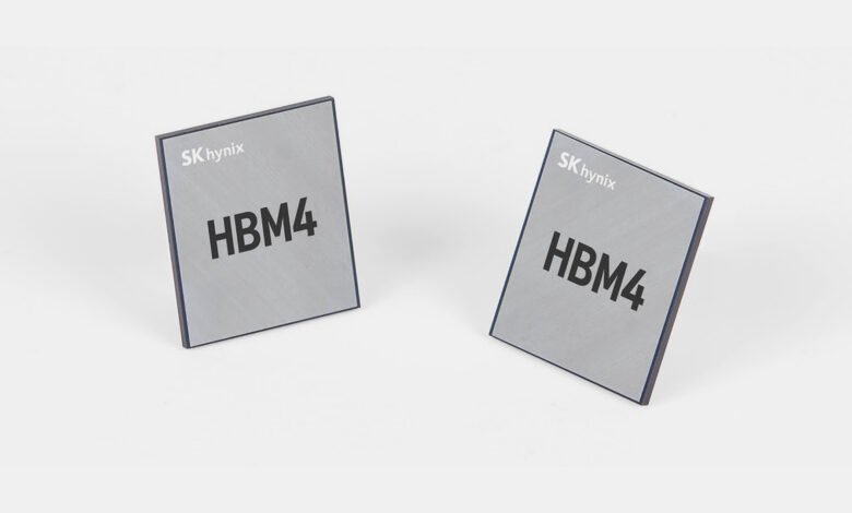
SK hynix Unveils HBM4: 2,048-Bit Interface for Next-Gen AI Accelerators
▼ Summary
– SK hynix has completed development of its HBM4 memory and prepared it for high-volume manufacturing.
– The HBM4 stacks exceed JEDEC performance specifications by 25% with a 10 GT/s data transfer rate and 2,048-bit I/O interface.
– The memory uses specially designed DRAM dies built on a 1b-nm process technology and the proven MR-MUF packaging method.
– SK hynix did not disclose specific details like layer count, capacity, or base die technology, though 12-Hi 36 GB devices are speculated.
– The company is ready for mass production but has not announced when volume production will begin.
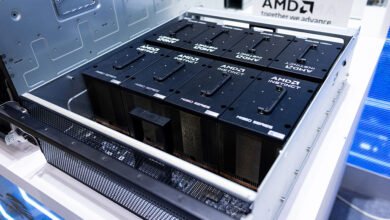
SK hynix has officially completed development of its next-generation HBM4 memory, positioning the technology for high-volume manufacturing. The company announced that its HBM4 stacks exceed JEDEC performance standards by 25%, setting a new benchmark for future AI accelerators expected from industry leaders like AMD, Broadcom, and Nvidia by 2026.
A standout feature of SK hynix’s HBM4 is its 2,048-bit interface, marking the first time the HBM bus width has doubled since 2015. This design supports a data transfer rate of 10 GT/s, significantly outpacing the official JEDEC specification of 8 GT/s. The memory stacks utilize advanced DRAM dies fabricated on a mature 1b-nm process node, balancing performance with manufacturing reliability.
The company continues to rely on its proprietary Advanced Mass Reflow Molded Underfill (MR-MUF) packaging technique. This method allows multiple memory chips to be stacked on a base substrate and bonded in a single reflow step. Mold material is then injected to fill gaps between layers, enhancing structural integrity and thermal management. This approach is particularly critical for maintaining the specified height and improving heat dissipation in power-intensive 12-high stack configurations.
Joohwan Cho, Head of HBM Development at SK hynix, emphasized the significance of this milestone, stating that timely delivery of products meeting customer demands for performance, power efficiency, and reliability will help the company maintain a competitive edge.
While specific details regarding layer count and capacity remain undisclosed, industry speculation points to 12-high 36 GB stacks likely destined for use in Nvidia’s upcoming Rubin data center GPUs. It is also unclear whether initial HBM4 products will incorporate 12FFC+ or N5-class base logic dies from TSMC.
Notably, SK hynix is not alone in pushing beyond JEDEC’s baseline specifications. Micron is sampling HBM4 devices rated at 9.2 GT/s, and Rambus has developed a memory controller capable of 10 GT/s speeds. This trend suggests that AI accelerator manufacturers may be seeking performance headroom for future design flexibility and reliability.
Justin Kim, President and Head of AI Infrastructure at SK hynix, highlighted the company’s readiness for mass production, calling HBM4 a turning point in overcoming AI infrastructure limitations. He reaffirmed SK hynix’s commitment to becoming a full-stack AI memory provider, delivering high-quality, performance-diverse products tailored for the demands of the AI era.
(Source: Tom’s Hardware)