Vision AI Accelerates Chip Debugging
▼ Summary
– Integrated circuit chips are becoming more complex, driving the need for advanced design processes that maintain productivity and quality despite physical and workforce challenges.
– Artificial intelligence is transforming electronic design automation by enabling new approaches like predictive modeling and natural language interaction, shifting problem-solving earlier in the design cycle.
– Physical verification, particularly design rule checking (DRC), is a critical bottleneck in chip design, with traditional late-stage verification causing costly delays due to millions of errors.
– AI-powered DRC tools like Siemens’ Calibre Vision AI use machine learning to cluster billions of errors into manageable groups, speeding up analysis and enabling collaborative, real-time debugging across teams.
– AI integration in DRC reduces the expertise gap by automating complex analyses, allowing less experienced designers to achieve expert-level results and significantly cutting debug time by at least half in real-world applications.
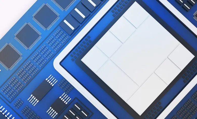
Integrated circuits are the silent engines of modern innovation, powering everything from advanced smartphones to autonomous vehicles and medical breakthroughs. As these chips grow more intricate, the task of designing them becomes exponentially more difficult. Engineers now face immense pressure to deliver higher performance while navigating a labyrinth of design constraints and manufacturing rules. The challenge isn’t just technical; it involves tight deadlines, workforce limitations, and the relentless demand for flawless reliability.
A transformative shift is underway within electronic design automation, where artificial intelligence is reshaping traditional methodologies. AI isn’t merely accelerating existing processes, it’s enabling entirely new approaches to chip development. From predicting manufacturing defects to optimizing circuit layouts, machine learning algorithms help identify risks and streamline workflows that once required extensive manual effort. This synergy between human skill and computational intelligence allows problems to be detected and resolved much earlier, improving both product quality and development speed.
Physical verification represents one of the most demanding stages in chip design. Design rule checking ensures a chip’s layout adheres to strict manufacturing guidelines, verifying that every transistor, wire, and connection meets precise specifications. With contemporary chips incorporating billions of components across multiple layers, the number of potential errors has exploded. Traditional verification methods, applied late in the design cycle, often uncover millions of violations, leading to significant delays and cost overruns.
To address this, many teams adopt a “shift-left” strategy, performing verification concurrently with design. However, analyzing unfinished layouts generates colossal datasets, sometimes billions of preliminary errors, that can overwhelm engineering teams. Manually sifting through these alerts is impractical, forcing designers to rely on ad-hoc methods like error caps and informal sharing of screenshots. These workarounds are inefficient and increase the risk of overlooking critical, system-wide issues.
Artificial intelligence offers a powerful solution to this data deluge. Modern AI-driven systems apply computer vision and machine learning to rapidly process and categorize enormous volumes of design violations. Instead of presenting engineers with an endless list of individual errors, these tools group related issues into clusters, highlighting systematic problems and root causes. This intelligent clustering transforms weeks of manual analysis into a guided, minutes-long investigation, allowing teams to resolve hundreds of issues with a single corrective action.
Collaboration is another area where AI brings substantial improvements. Next-generation verification platforms provide shared, interactive workspaces where teams can annotate results, assign tasks, and exchange precise analytical views. Dynamic bookmarks preserve filter settings, zoom levels, and annotations, ensuring that all team members work from the same contextual information. This eliminates the confusion of exchanging static reports and reduces repetitive clarification cycles.
Siemens’ Calibre Vision AI exemplifies this advanced approach to design rule checking. The platform combines a high-speed processing engine with sophisticated AI clustering to manage billions of layout errors efficiently. It presents data through intuitive heat maps and layer-controlled visualizations, helping engineers quickly identify trouble spots. In one documented case, the system condensed 600 million errors from 3,400 checks into just 381 actionable groups, slashing debug time by more than half.
The platform also helps bridge the experience gap between junior and senior engineers. Its algorithms replicate the analytical patterns of expert designers, enabling less experienced team members to diagnose complex issues confidently. Integrated generative AI assistants allow designers to ask natural-language questions about design rules or analysis signals, accelerating both training and daily problem-solving.
Real-world adoption of AI-enhanced verification is yielding measurable benefits. Several leading semiconductor firms report cutting debug efforts by at least fifty percent. In benchmark tests, error files that previously required hours to load and analyze are now processed in minutes. One test involving 3.2 billion errors from over 380 rule checks was clustered into 17 meaningful groups in just five minutes, a task that would have taken weeks using conventional methods.
Looking forward, the role of AI in chip design will only expand. As semiconductor complexity increases, intelligent tools that enhance productivity, collaboration, and accuracy will become indispensable. By merging engineering creativity with machine learning, platforms like Calibre Vision AI are not only keeping pace with innovation but turning design complexity into a strategic advantage. The future of chip verification lies in this seamless integration of human insight and artificial intelligence, ensuring that groundbreaking ideas can transition from concept to silicon more rapidly than ever.
(Source: Spectrum)