NSRAM: Artificial Neuron Built on a Silicon Chip
▼ Summary
– AI interactions consume significant energy because GPUs in data centers use up to 1,000 watts each, running continuously, while the human brain is about one million times more energy efficient for comparable tasks.
– Neuromorphic engineering aims to mimic biological neurons and synapses with electronics, but previous attempts required complex circuits of many transistors, limiting scalability and efficiency.
– Researchers accidentally discovered that a single MOSFET with a floating bulk terminal can act as an artificial neuron, producing a current spike and hysteresis through impact ionization and hole accumulation.
– The same MOSFET can also function as an artificial synapse by trapping charge in the gate dielectric via controlled bulk voltage, allowing stable, adjustable conductance.
– These single-transistor neurons and synapses, called NSRAM, are fully compatible with existing silicon manufacturing, achieve 100% yield with near-zero variability, and could enable energy-efficient brain-inspired chips for AI.
The average person interacts with artificial intelligence multiple times daily,querying a large language model, accepting a LinkedIn suggestion, watching a YouTube recommendation, or following a Google Maps traffic reroute. What often goes unnoticed, however, is the staggering energy cost behind each of those interactions.
AI data processing demands immense computational power, typically housed in vast data centers packed with thousands of GPUs. These processors can execute trillions of operations per second but consume up to 1,000 watts each. For perspective, a modern smartphone uses less than 1 watt. That puts a single GPU on par with a vacuum cleaner or dishwasher,except data-center chips run nonstop, 24/7. The core inefficiency stems from GPUs simulating artificial neural networks through software and billions of transistors, which requires moving enormous volumes of data. Worse, these simulated neurons lack the sophisticated computing behaviors of biological neurons, which power the most energy-efficient computer known: the human brain.
The brain is roughly one million times more energy efficient than current AI systems for comparable tasks. To bridge this gap, researchers have pursued neuromorphic engineering, a radically different computing paradigm that builds electronic components mimicking neurons and synapses. Much effort has gone into developing experimental devices, but they remain unreliable for large-scale systems. Other approaches interconnect dozens of CMOS transistors to simulate a single neuron or synapse, but this consumes so much chip area that scaling up to compete with GPUs seems doubtful.
Then, unexpectedly, a breakthrough emerged. Last year, researchers discovered that an ordinary CMOS transistor,not even a high-performance one,could function as both an artificial neuron and a synapse all by itself. This accidental finding could dramatically lower AI’s environmental footprint.
Modern digital electronics relies on MOSFETs (metal-oxide-semiconductor field-effect transistors) to produce binary ones and zeros. A classic MOSFET has four terminals: source, drain, gate, and a bulk terminal that typically connects to the chip’s underside and is often ignored. When voltage is applied to the gate with the bulk grounded, charge carriers form a conductive channel, switching the transistor on. This response works well for logic circuits but poorly mimics neurons.
Biological neurons fire an action potential when their voltage crosses a threshold, then quickly return to a resting state. Artificial neurons need to produce a sudden current spike with hysteresis,different activation and relaxation voltages. Artificial synapses require adjustable conductance that changes linearly and remains stable. No single MOSFET operating normally can do either.
But in 2024, a student in the lab forgot to connect the bulk terminal of a MOSFET while measuring a memory circuit. He observed a sudden current increase with high nonlinearity that self-relaxed,a promising neuronlike behavior. Further investigation revealed the secret: a hidden bipolar junction transistor inside every MOSFET.
Normally, impact ionization produces electron-hole pairs. With the bulk grounded, holes are removed harmlessly. But with the bulk floating, holes accumulate, raising the bulk voltage. Once it reaches a threshold (around 0.7 volts), the hidden bipolar transistor activates, causing an abrupt current spike. The spike fades when drain voltage drops, holes recombine, and the device relaxes,mimicking a biological neuron’s integrate-and-fire cycle.
Initially, behavior varied between transistors. By adding a second MOSFET to control the bulk resistance, the team achieved perfect uniformity across all devices. Every transistor fired at the same voltage with negligible variability. Testing over 10 million cycles showed zero failures.
The same MOSFET also works as a synapse. At specific bulk resistance values, impact ionization traps charge in the gate dielectric, altering conductance. A negative bulk-source voltage drives electrons into the dielectric (decreasing conductance); a positive voltage pushes holes in (increasing it). This stable, adjustable conductance is exactly what an artificial synapse needs.
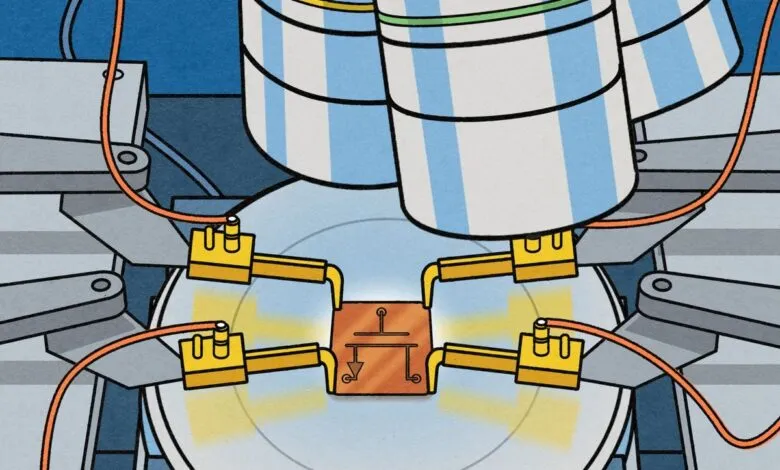
Together, these devices form a neurosynaptic random-access memory (NSRAM) cell. In a simple circuit, three synapse MOSFETs with programmed conductances receive voltage spikes. Their output currents converge at a neuron MOSFET’s drain. If enough spikes arrive quickly, the bulk voltage triggers a spike,exactly like biological integrate-and-fire behavior.
The advantage is clear: one or two transistors replace the dozens or hundreds currently needed. And unlike experimental technologies, NSRAM is fully compatible with existing silicon manufacturing, achieving 100% yield with near-zero variability.
Building functional brain-inspired chips will require improved computer models, circuit simulations, peripheral circuitry design, and multiple fabrication rounds. But the payoff could be dramatically more energy-efficient AI hardware. Initially suited for edge-AI tasks in battery-powered devices, these chips might eventually scale to compete with state-of-the-art GPUs,potentially transforming AI’s environmental impact.
(Source: Ieee.org)