Google, Broadcom, MediaTek, Marvell Form AI Chip Alliance to Rival Nvidia
▼ Summary
– Google is building the AI industry’s most diversified custom chip supply chain, involving four design partners and a roadmap from current chips to 2nm processors in 2027.
– Its strategy explicitly splits the next-generation TPU v8, with Broadcom designing a training chip and MediaTek designing a lower-cost inference chip.
– Google’s custom silicon, led by the new Ironwood inference TPU, is positioned as a direct challenge to Nvidia’s dominance in AI inference workloads.
– The company is pursuing multiple inference chip paths simultaneously to gain cost advantages and reduce supply chain dependence on any single partner.
– Google’s total expected TPU shipments are projected to scale from 4.3 million units in 2026 to over 35 million by 2028, with significant commitments from partners like Anthropic.
Google is constructing the most varied and resilient supply chain for custom artificial intelligence chips in the industry, a strategic move directly challenging Nvidia’s stronghold on the critical AI inference market. This multi-partner approach, detailed ahead of the Google Cloud Next conference, involves distinct design collaborations with Broadcom, MediaTek, and Marvell, alongside a foundational manufacturing partnership with TSMC. The roadmap extends from current deployments to advanced 2-nanometer processors slated for late 2027, aiming to secure cost and performance advantages at a massive scale.
The immediate focus is on Google’s Ironwood TPU, the seventh generation and first built specifically for inference workloads. It reportedly delivers ten times the peak performance of its predecessor, the TPU v5p, and features 192GB of HBM3E memory per chip. These liquid-cooled chips can scale into superpods of over 9,000 units. Google is now shipping Ironwood to cloud customers, with plans to produce millions this year. Major commitments include a deal with Anthropic for up to one million units and a rental arrangement with Meta.
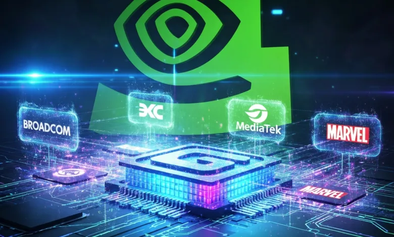
This ambitious strategy relies on a carefully segmented, four-partner design ecosystem. Each company plays a specialized role to foster competition and reduce supply chain risk. Broadcom, which signed a long-term supply agreement in early April, handles high-performance variants. It is designing the next-generation TPU v8 training chip, codenamed “Sunfish,” for TSMC’s 2nm node. Broadcom currently holds over 70% of the custom AI accelerator market.
MediaTek is tasked with the cost-optimized inference version of the TPU v8, known as “Zebrafish.” Its involvement began with peripheral components on Ironwood, where its designs are 20 to 30% cheaper. By explicitly splitting the v8 line between Broadcom for training and MediaTek for inference, Google gains significant negotiating leverage.
Marvell Technology is in discussions to become a third design partner, potentially developing a memory processing unit and a new inference-focused TPU. If finalized, Google plans to produce nearly two million of these memory units. Nvidia itself invested $2 billion in Marvell earlier this year, highlighting the interconnected nature of this evolving ecosystem. Intel rounds out the group with a separate multi-year deal to supply Xeon processors and infrastructure units for Google’s data centers, supporting the layers surrounding the core AI accelerators. All custom silicon is fabricated by TSMC, creating a unified manufacturing backbone.
The entire program is driven by a fundamental economic shift in AI computing. While training a model is a singular, intensive event, inference is continuous, scaling with every user query and API call. For a company serving billions of daily AI interactions, the cost per inference becomes the defining economic metric. Nvidia’s GPUs, fortified by the CUDA software ecosystem, remain formidable for training. However, inference workloads are more predictable and repetitive, making them ideal for the fixed-function optimization of custom silicon. A purpose-built chip that costs less per query can win on economics, even without matching a GPU’s versatility.
This explains Google’s parallel investment in multiple inference paths. Ironwood addresses current needs, MediaTek’s Zebrafish targets the next generation at lower cost, and Marvell’s proposed chips would add another option. This redundancy builds crucial optionality, insulating Google from the pricing, capacity, and strategic risks of dependency on any single supplier.
The scale of Google’s ambition is reflected in its projections. Total expected TPU shipments could reach 4.3 million units in 2026, scaling to over 35 million by 2028. Anthropic’s commitment alone represents a significant portion, granting it access to gigawatts of next-generation TPU compute starting in 2027. Analysts estimate Broadcom’s AI revenue from its Google and Anthropic relationships could hit $42 billion in 2027. The broader custom ASIC market is growing rapidly, projected to outpace GPU shipment growth significantly through this decade.
Google is not alone in this pursuit. Amazon, Microsoft, and others are developing their own custom silicon. Yet, Google’s multi-partner, multi-generation blueprint is notably comprehensive. The challenge to Nvidia is not that one Google chip will outright outperform its GPUs. Instead, Google is building a system where a portfolio of optimized chips collectively reduces the share of its AI compute running on Nvidia hardware. Nvidia’s response has been to embed itself within this custom chip ecosystem through investments and programs like NVLink Fusion.
Google’s fundamental bet is that controlling its own silicon destiny across multiple partners will yield a compounding cost advantage in inference. The economics increasingly favor custom silicon for this workload, and no company handles more inference volume than Google. Its diversified supply chain and dual-track roadmap form the infrastructure for a competitive position intended to strengthen with every query served.
(Source: The Next Web)