The Evolution of NAND Flash Memory
▼ Summary
– NAND flash memory is evolving toward cheaper, faster 3D NAND with over 500 layers and speeds reaching 4800 MT/s.
– Major manufacturers are increasing layer counts and shrinking cell sizes to enhance capacity, performance, and cost efficiency.
– By 2027, 4800 MT/s speeds will standardize, enabling PCIe 5.0/6.0 SSDs to maximize bandwidth with fewer channels.
– Vendors aim to achieve 1-2 Tb die capacities by 2026-2027, leveraging QLC NAND for high-density storage despite challenges.
– Future advancements rely on vertical scaling and hybrid bonding, though higher manufacturing complexity and costs remain barriers.
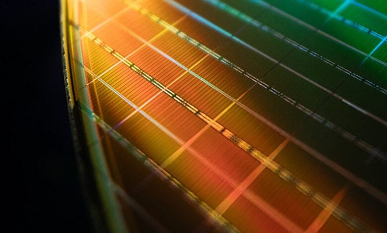
Decades of technological evolution have transformed NAND flash memory from an expensive rarity into a ubiquitous element of modern devices. Whether in consumer electronics or data centers, NAND flash is essential. In its early days, NAND was costly, though it was already faster than traditional spinning disks. As the technology matured, it became more affordable and widespread. Looking ahead, significant advancements are on the horizon, with the industry progressing towards 500-layer stacks and 4800 MT/s interfaces by 2027. This evolution promises not only denser storage but also faster and more efficient performance.
The Race to 500 Layers
Manufacturers are continuously working to enhance 3D NAND technology by increasing layer counts while reducing the physical size of memory cells. Currently, 3D NAND devices feature around 200 layers, such as Kioxia’s 218-layer, Micron’s 232-layer, and Samsung’s 286-layer offerings. This evolution reflects a strategic approach to meet the growing demand for higher capacity, greater performance, and more compact storage solutions. As manufacturers push toward 500 layers by 2027, the potential for even more advanced storage solutions becomes increasingly feasible.
Speed: The Competitive Edge
Speed is a critical factor in NAND development. By early 2023, major players like Kioxia, Micron, and Samsung had established a baseline interface speed of 2400 MT/s for TLC products. Samsung then introduced an intermediate V9T TLC with a speed of 3000 MT/s in 2024, showcasing its commitment to advancing its own-brand products. By 2027, industry leaders anticipate reaching an interface speed of 4800 MT/s, which will mark a new standard for high-performance storage solutions.
Implications of High-Speed NAND
The move towards higher speeds presents practical implications. To fully utilize a PCIe 5.0 x4 interface, which offers up to 15.75 GB/s of effective bandwidth, SSD controllers must adapt. Current technology requires eight channels at 2400 MT/s to saturate this interface, but with advancements to 3600 MT/s or even 4800 MT/s, fewer channels will be necessary. The introduction of PCIe 6.0 promises even greater throughput, although the adoption of such interfaces in consumer devices remains to be seen.
Layer Counts and Die Capacities
By 2026, leading 3D NAND manufacturers plan to offer 1 Tb and 2 Tb die capacities, particularly for QLC products. Although some 2 Tb devices have been announced, they have yet to hit the market. Despite the rising layer counts, manufacturers are cautious about exceeding 2 Tb per device, likely due to cost considerations. The roadmap indicates a convergence towards 300–500-layer stacks, enhancing storage density and performance.
The Competitive Landscape
Companies like Kioxia, Micron, Samsung, SK Hynix, and YMTC are at the forefront of 3D NAND development. Kioxia and Western Digital, for example, have a strong roadmap with their BiCS series, targeting over 300 layers by 2027. Micron’s advancements with their B68S IC, achieving 3600 MT/s, position them as leaders in enthusiast-grade SSDs. Samsung, with its vertically integrated approach, aims to reach over 400 layers with its V10T IC by 2026. Meanwhile, SK hynix plans to unveil a 500-layer, 4800 MT/s node by 2027, hinting at significant vertical scaling.
Looking Ahead
The future of 3D NAND is defined by aggressive vertical scaling, faster interfaces, and a push towards higher per-die capacities. By 2027, 4800 MT/s interface speeds and layer stacks of 300–500 will become the norm. Despite challenges in yield and cost increases due to advanced processing techniques, the industry’s trajectory is clear. The move to hybrid bonding and complex manufacturing processes will further shape the future, offering faster speeds and more efficient storage solutions. The 3D NAND horizon is bright, with continued innovation paving the way for next-generation storage technology.
(Source: Tom’s Hardware)