Intel’s Bold Bid to Regain Chip Supremacy
▼ Summary
– Intel’s Fab 52 semiconductor plant in Arizona has begun producing its first chips after four years of construction.
– The facility will manufacture new CPUs using Intel’s advanced 18A process technology, which aims to create more powerful and efficient chips.
– The fab opening is a critical opportunity for Intel to demonstrate it can produce world-class chips at scale, following a recent $8.9 billion investment from the U.S. government.
– Intel showcased the highly automated fab, featuring robots, large lithography machines, and strict anti-contamination measures like bunny suits and rapid air recycling.
– The company’s success depends on whether these new semiconductors can attract both traditional hardware customers and AI companies needing advanced chips for data centers.
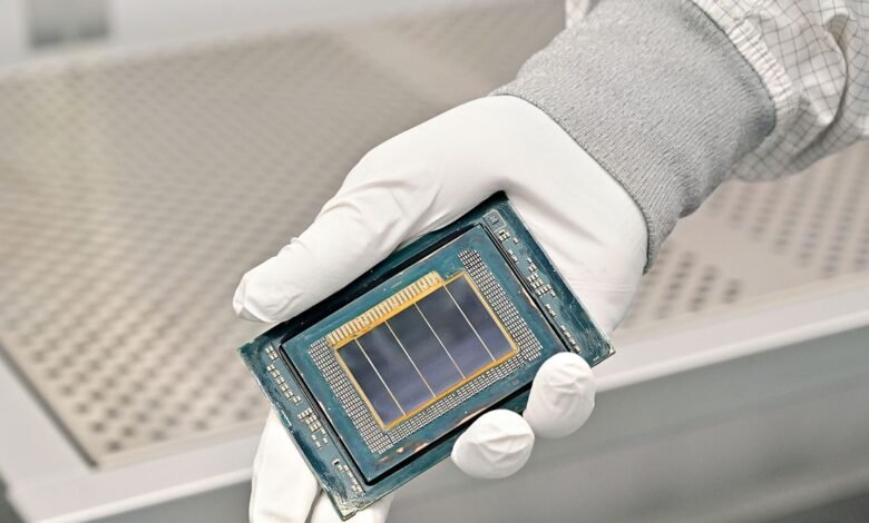
After a four-year construction period, Intel has officially announced that its Fab 52 semiconductor facility in Chandler, Arizona is now producing its first chips. The company also provided new details about its upcoming Panther Lake and Clearwater Forest CPUs, which will be manufactured at the plant using Intel’s advanced 18A process technology. This milestone arrives just weeks after the U.S. government acquired a 9.9% stake in Intel through an $8.9 billion stock transaction, signaling strong federal backing for the company’s efforts to reclaim leadership in the global semiconductor market.
Last month, Intel hosted a select group of analysts, business partners, and journalists for an exclusive tour of Fab 52. The visit offered a rare look into the highly automated environment of modern chip fabrication, where robotic systems handle most operations and massive lithography machines, some as large as school buses, etch intricate microscopic designs onto silicon wafers. All personnel, including guests, are required to wear specialized anti-contamination gear, often referred to as “bunny suits,” along with booties, goggles, and gloves. According to Intel, the air inside the facility is completely refreshed every six seconds to maintain an ultra-clean environment.
Such extreme measures are essential because even a single particle of dust can permanently ruin a silicon wafer, the foundational component of virtually all computing devices. Intel has indicated that Fab 52 has been technically operational since July, but the public unveiling was timed to showcase the company’s progress at a pivotal moment. The facility is designed specifically for the 18A manufacturing process, which Intel claims will deliver chips with superior performance and energy efficiency.
Intel’s future success may depend on its ability to produce semiconductors that not only meet the needs of traditional hardware and computer clients but also appeal to AI firms investing heavily in advanced chips and data center infrastructure. During the recent tour, company executives emphasized that Fab 52 represents the most sophisticated chip manufacturing plant in operation today. Industry analysts acknowledge Intel’s historical strength in developing cutting-edge fabrication nodes. For example, the company made significant strides in the early 2010s with its 32-nanometer technology, a major leap at the time. Today, Intel’s latest chips are being produced at the 2-nanometer scale, underscoring the rapid pace of innovation in semiconductor manufacturing.
(Source: Wired)