Diamond Cooling: The Future of High-Performance Chips

▼ Summary
– Increasing computing power creates thermal challenges as heat builds up in nanometer-scale transistors, forcing performance throttling to prevent chip degradation.
– Diamond is an ideal heat-spreading material due to its high thermal conductivity and electrical insulation, but integrating it into chips was historically difficult due to high growth temperatures.
– Researchers developed a method to grow polycrystalline diamond coatings directly on semiconductor devices at low temperatures (around 400°C), preserving delicate chip components.
– In tests, diamond coatings reduced transistor temperatures by over 50°C and improved radio signal amplification fivefold, with potential applications in 3D-stacked CMOS chips.
– The technology addresses thermal bottlenecks in advanced chip architectures and is drawing industry interest for its ability to enable higher-performance electronics by managing heat more effectively.
Modern computing power is advancing at a breathtaking pace, enabling the shift from human-driven intelligence to sophisticated artificial intelligence systems. These powerful machines are no longer just tools; they are becoming active decision-makers that influence our daily lives and future direction. However, this incredible power comes with a significant challenge: managing the intense heat generated by today’s high-performance chips.
As transistors shrink to nanometer scales and operate at gigahertz speeds, electrons moving through circuits lose energy in the form of heat. Anyone who has felt a laptop or smartphone grow warm understands this phenomenon firsthand. The relentless drive to pack more transistors onto each chip has left little room for heat to dissipate effectively. Instead of spreading evenly across the silicon surface, thermal energy accumulates in concentrated hot spots that can reach temperatures dozens of degrees higher than surrounding areas. This excessive heat forces systems to throttle processor performance to prevent permanent damage to delicate chip components.
What began as a pursuit of miniaturization has evolved into an urgent battle against thermal constraints. This thermal management challenge spans every sector of electronics. High-performance processors demand increasingly dense power delivery, with some next-generation GPU servers projected to consume nearly 15 kilowatts. Communication systems push transistors to deliver stronger signals and faster data rates, while power electronics face efficiency limitations due to thermal barriers.
The solution might lie in an unexpected material: diamond. Rather than allowing heat to accumulate, researchers are exploring ways to distribute thermal energy immediately at its source, similar to how a cup of boiling water cools rapidly when poured into a swimming pool. Spreading heat internally would lower temperatures at critical circuit locations and enhance the effectiveness of traditional cooling methods. Achieving this requires integrating a highly thermally conductive material nanometers away from transistors without disrupting their precise electrical characteristics.
Diamond presents unique advantages for this application. It ranks among the most thermally conductive materials known, significantly outperforming copper while maintaining excellent electrical insulation properties. The historical challenge has been integrating diamond into chip manufacturing processes, as traditional diamond growth methods required temperatures exceeding 1,000°C – far too hot for delicate semiconductor devices.
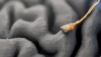
Recent breakthroughs at Stanford University have overcome this limitation. Researchers have developed a method to grow specialized diamond coatings directly on semiconductor devices at temperatures low enough to preserve sensitive chip components. These aren’t gem-quality diamonds but rather polycrystalline coatings just micrometers thick, specifically engineered for heat spreading applications.
The potential benefits are substantial. In early tests with gallium-nitride radio-frequency transistors, the diamond coating reduced device temperatures by over 50°C. At these lower operating temperatures, the transistors demonstrated five times better signal amplification performance in the X-band frequency range. The technology shows even greater promise for advanced CMOS chips, where researchers predict hot spots could become nearly 10°C hotter in future generations. This potential has attracted significant industry interest from major semiconductor manufacturers including Applied Materials, Samsung, and TSMC.
Understanding heat flow in chips begins at the transistor level, where electrical current meets resistance, generating thermal energy near the semiconductor surface. This heat travels upward through metal layers and insulation or downward through the semiconductor itself, depending on the chip architecture. Eventually, the heat reaches thermal interface materials designed to spread it before final dissipation through heat sinks, radiators, or liquid cooling systems.
Current cooling strategies focus primarily on improving heat sinks, fans, and radiators. More advanced approaches include liquid cooling through microfluidic channels and phase-change materials. Some high-performance computing systems even submerge entire servers in thermally conductive, electrically insulating fluids. While these methods represent important advances, they face limitations in cost, size, and effectiveness – particularly for compact devices like smartphones or emerging three-dimensional chip architectures that stack multiple silicon layers vertically.
The fundamental issue remains that chip materials generally conduct heat poorly, causing thermal energy to concentrate in localized hot spots. Elevated temperatures increase transistor leakage currents, wasting power and accelerating device aging. Traditional heat spreaders sit relatively far from heat generation sites, providing limited relief for these concentrated thermal zones. What’s needed is a heat-spreading technology that operates within nanometers of where heat originates.
The development of low-temperature diamond growth emerged from earlier research into diamond-based semiconductors. Single-crystal diamond possesses exceptional thermal conductivity – approximately six times greater than copper – along with a wide bandgap and remarkable electrical field tolerance. While attractive for transistor applications, scaling single-crystal diamond substrates to commercial wafer sizes presented significant challenges.
Researchers instead focused on growing diamond films directly on silicon wafers using methane and hydrogen reactions. Standard processes produced nanoscale diamond columns that eventually coalesced into thick polycrystalline films, but these often developed stress-related cracks. The breakthrough came from reimagining these polycrystalline coatings as integrated heat spreaders rather than standalone substrates.
Successful implementation required solving multiple technical challenges. The diamond needed to grow within nanometers of transistors, spread heat in both vertical and lateral directions, and integrate seamlessly with existing chip materials. Diamond’s electrical insulation properties and low dielectric constant made it particularly suitable, as it wouldn’t significantly degrade signals passing through nearby interconnects.
The research team developed a modified growth process that produced large-grained polycrystalline diamond at just 400°C – a temperature compatible with CMOS circuitry. This involved adding oxygen to the reaction mixture, which continuously removed non-diamond carbon deposits that would otherwise form conductive soot.
Even with successful diamond growth, another obstacle remained: thermal boundary resistance. This “phonon bottleneck” occurs when heat-carrying phonons – quantized lattice vibrations – encounter resistance at material interfaces. Through careful interface engineering, researchers discovered that intermixing between diamond and silicon nitride naturally formed silicon carbide, which acted as a thermal bridge that significantly improved heat transfer efficiency.
Gallium nitride high-electron-mobility transistors (HEMTs) provided an ideal test platform. These devices generate heat very close to their surface, making any thermal interference immediately apparent. By completely surrounding HEMTs with diamond coatings grown below 400°C, researchers achieved temperature reductions up to 70°C despite minor high-frequency performance trade-offs.
The technology shows equal promise for CMOS applications, particularly in three-dimensional chip stacks where thermal management becomes increasingly challenging. In collaboration with Stanford colleagues, researchers developed “thermal scaffolding” concepts incorporating nanometer-thick diamond layers within dielectric materials above transistors. These horizontal heat spreaders connect to vertical thermal pillars made of copper or additional diamond, creating continuous thermal pathways through multiple chip layers.
Simulations using dummy heaters to mimic real computational workloads demonstrated temperature reductions to one-tenth of values observed without thermal scaffolding. The approach becomes increasingly critical as chip architectures incorporate more computing tiers, with AI accelerators exceeding five layers likely surpassing standard temperature limits without such interventions.
Current research focuses on addressing remaining technical hurdles, particularly achieving atomically flat diamond surfaces. Through industry partnerships and programs like DARPA’s Threads initiative, researchers are validating low-temperature diamond integration in manufacturing environments. Early results are promising, guiding refinements in growth processes and integration techniques scheduled for implementation over the coming years.
The vision extends beyond gallium nitride devices to silicon computational chips, with established collaborations through the Stanford SystemX Alliance and Semiconductor Research Corporation. The universal nature of thermal challenges in chip manufacturing has fostered unprecedented cooperation among typically competitive companies. If successful, diamond-based thermal management could follow the trajectory of other once-radical semiconductor innovations, becoming a standard enabling technology for future electronics no longer constrained by thermal limitations.
(Source: Spectrum)