Part 2: The Making of Magic – Semiconductor Manufacturing Process
Welcome back to our quick-read series on the semiconductor industry! Last time, we laid the groundwork by exploring what semiconductors are and their fascinating history. Now, let’s roll up our sleeves and dive into the heart of the action – the semiconductor manufacturing process.
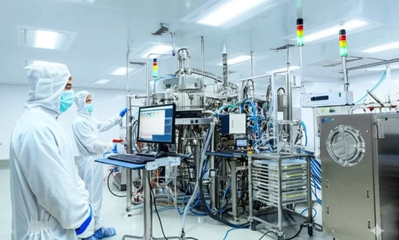
Wafer Manufacturing: The Foundation
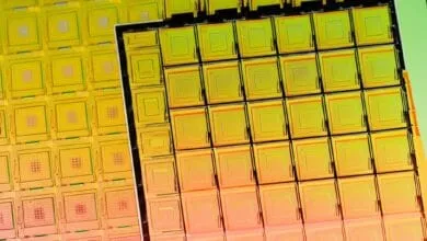
Every great structure needs a solid foundation, and in the world of semiconductors, that foundation is the wafer. Wafer manufacturing kicks things off by growing a single crystal of silicon. Imagine a seed crystal being carefully lowered into a vat of molten silicon, then slowly pulled out as the silicon solidifies around it – this is the Czochralski process. Once the crystal is grown, it’s sliced into thin, circular wafers, much like cutting a loaf of bread. These wafers are then polished to a mirror-like finish to ensure they’re ready for the next steps.
Photolithography: Painting with Light
Here’s where things get truly fascinating. Photolithography is essentially the process of “drawing” the intricate patterns of circuits onto the wafer. It’s like using light as a paintbrush. A photomask, which is kind of like a stencil with the circuit design etched into it, is placed over the wafer. Then, ultraviolet light is shone through the mask, transferring the pattern onto a light-sensitive coating called photoresist. This allows the desired pattern to be imprinted with incredible precision.
Etching and Doping: Shaping and Enhancing
Now that the pattern is on the wafer, it’s time to etch. Etching involves using chemicals or plasma to remove the areas not protected by the photoresist, carving out the tiny structures that will form the transistors and other components. After etching, doping comes into play. This is when impurities are introduced into the silicon to alter its electrical properties. By carefully controlling where and how much doping is done, we can create the P-type and N-type regions needed for the semiconductor devices to function.
Packaging and Testing: The Final Touches
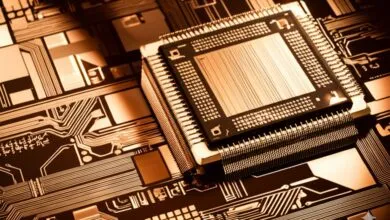
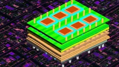
Once the wafer has been through all these processes, it’s time to package the individual chips and put them through their paces with rigorous testing. Packaging involves protecting the delicate chip and providing a way for it to connect with the outside world. This could be as simple as placing it in a plastic package with metal pins or as complex as advanced 3D packaging for cutting-edge applications. Testing ensures that each chip meets the required specifications and will perform reliably in real-world conditions.
Join us next time as we venture into the realm of core technologies and trends in the semiconductor industry. We’ll explore how innovation is driving the future of this fascinating field.
Quick-Series Navigator:
- Introductory post
- Part 1: Semiconductor Basics
- Part 2: The Making of Magic – Semiconductor Manufacturing Process
- Part 3: Core Technologies and Trends in the Semiconductor Industry
- Part 4: Key Players in the Semiconductor Industry
- Part 5: Market Trends and Future Outlook